


Flip Chip
Flip chip, also known as controlled collapse chip connection or its acronym, C4, is a method for interconnecting semiconductor devices, such as IC chips and microelectromechanical systems (MEMS), to external circuitry with solder bumps that have been deposited onto the chip pads. The solder bumps are deposited on the chip pads on the top side of the wafer during the final wafer processing step. In order to mount the chip to external circuitry (e.g., a circuit board or another chip or wafer), it is flipped over so that its top side faces down, and aligned so that its pads align with matching pads on the external circuit, and then the solder is flowed to complete the interconnect. This is in contrast to wire bonding, in which the chip is mounted upright and wires are used to interconnect the chip pads to external circuitry.
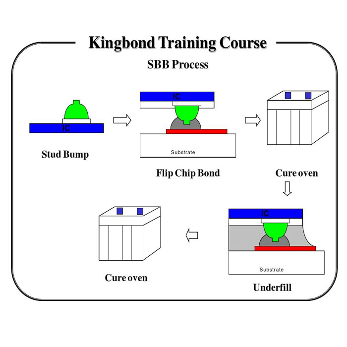
Process steps:
- Integrated circuits are created on the wafer
- Pads are metalized on the surface of the chips
- Solder dots are deposited on each of the pads
- Chips are cut
- Chips are flipped and positioned so that the solder balls are facing the connectors on the external circuitry
- Solder balls are then remelted (typically using hot air reflow)
- Mounted chip is “underfilled” using an electrically-insulating adhesive
In typical semiconductor fabrication systems chips are built up in large numbers on a single large wafer of semiconductor material, typically silicon. The individual chips are patterned with small pads of metal near their edges that serve as the connections to an eventual mechanical carrier. The chips are then cut out of the wafer and attached to their carriers, typically via wire bonding such as Thermosonic Bonding. These wires eventually lead to pins on the outside of the carriers, which are attached to the rest of the circuitry making up the electronic system.
Processing a flip chip is similar to conventional IC fabrication, with a few additional steps.Near the end of the manufacturing process, the attachment pads are metalized to make them more receptive to solder. This typically consists of several treatments. A small dot of solder is then deposited on each metalized pad. The chips are then cut out of the wafer as normal.
To attach the flip chip into a circuit, the chip is inverted to bring the solder dots down onto connectors on the underlying electronics or circuit board. The solder is then re-melted to produce an electrical connection, typically using an ultrasonic or alternatively reflow solder process. This also leaves a small space between the chip’s circuitry and the underlying mounting. In most cases an electrically-insulating adhesive is then “underfilled” to provide a stronger mechanical connection, provide a heat bridge, and to ensure the solder joints are not stressed due to differential heating of the chip and the rest of the system.
Recently, high-speed mounting methods evolved through a cooperation between Reel Service Ltd. and Siemens AG in the development of a high speed mounting tape known as ‘MicroTape. By adding a tape-and-reel process into the assembly methodology, placement at high speed is possible, achieving a 99.90% pick rate and a placement rate of 21,000 cph (components per hour), using standard PCB assembly equipment.
The resulting completed flip chip assembly is much smaller than a traditional carrier-based system; the chip sits directly on the circuit board, and is much smaller than the carrier both in area and height. The short wires greatly reduce inductance, allowing higher-speed signals, and also conduct heat better.
Flip chips have several disadvantages. The lack of a carrier means they are not suitable for easy replacement, or manual installation. They also require very flat surfaces to mount to, which is not always easy to arrange, or sometimes difficult to maintain as the boards heat and cool. Also, the short connections are very stiff, so the thermal expansion of the chip must be matched to the supporting board or the connections can crack.The underfill material acts as an intermediate between the difference in CTE of the chip and board.
The process was originally introduced commercially by IBM in the 1960s for individual transistors and diodes packaged for use in their mainframe systems.DEC followed IBM’s lead, but was unable to achieve the quality they demanded, and eventually gave up on the concept. It was pursued once again in the mid-90s for the Alpha product line, but then abandoned due to the fragmentation of the company and subsequent sale to Compaq. In the 1970s it was taken up by Delco Electronics, and has since become very common in automotive applications.
Since the flip chip’s introduction a number of alternatives to the solder bumps have been introduced, includinggold balls or molded studs, electrically conductive polymer and the “plated bump” process that removes an insulating plating by chemical means. Flip chips have recently gained popularity among manufacturers of cell phones, pagers and other small electronics where the size savings are valuable.